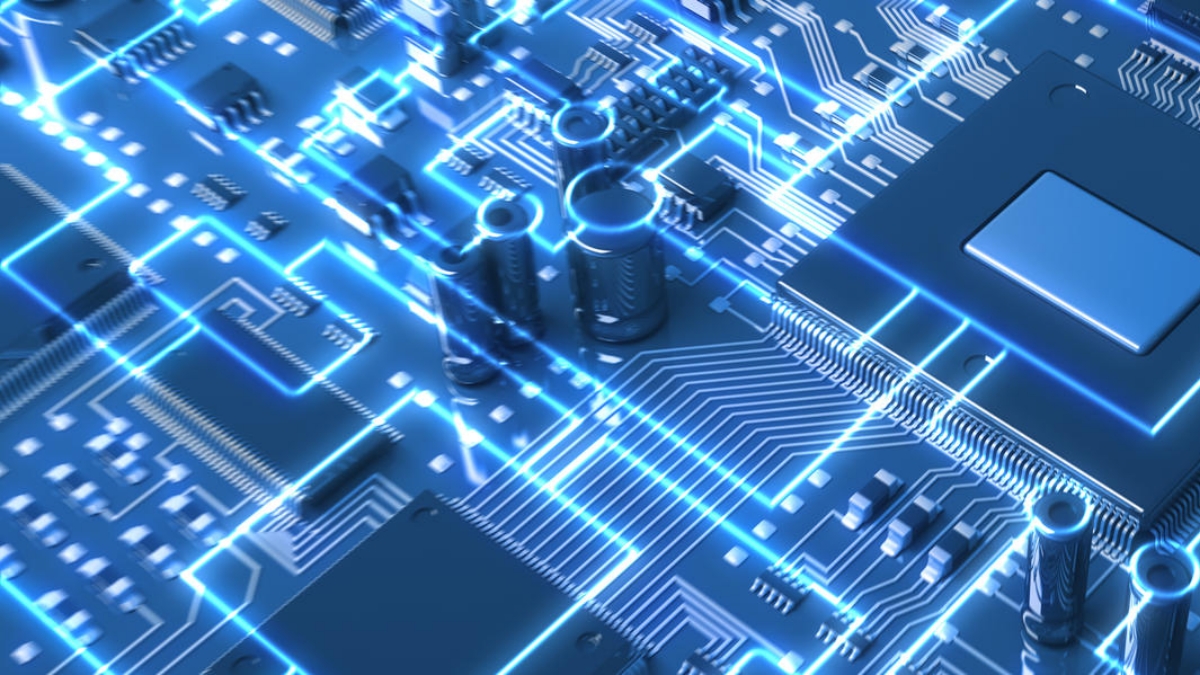
The process of making an idea into reality begins from estimation, preparation and prototyping and ends with manufacturing of the product. One of the stages in product manufacturing is the design of a printed circuit board (PCB). PCB is the ‘brains’ of your device, it connects electronic components and allows your device to operate. Here is some information about PCB that will allow you to understand this process better. In case you need PCB design and manufacturing professionals.
Table of Contents
General Information About PCB
The size of PCB depends on the size of your product. Obviously, the PCB should fit in the ‘body’ of your device. The number of PCB layers depends on your product as well, but you should note that a more complex and layered PCB requires more costs. Manufacturing PCB also involves such information as material, thickness, color, surface finish, copper weight, etc. All these nuances can be determined by professional companies.

Design Process
The PCB design process involves a range of stages. Here’s a brief description of each. Firstly, electronic designers create a schematic file in which the components of PCB and their interrelation is described. For example, the schematic includes component specifications, their physical dimensions, placement, and other details. This process requires relevant software tools. Luckily, there are numerous software tools to choose from, e.g. Quadcept, Altium, PADs, etc. This stage is highly important since the schematic is a reference file for the actual PCB.
The second step is the creation of a PCB layout. It is more complicated than the schematic since the layout allocates the actual components of PCB regarding the layers. In order to create the layout, electronic designers divide the PCB into sections in accordance with the functionality of the device and group relevant components to further locate them where necessary. Locations of the components are important and must align with the functionality of the device. In addition, designers place components in a way that prevents unnecessary interference between them. All the information about components and their exact location is contained in a file that will be used in manufacturing of the PCB.

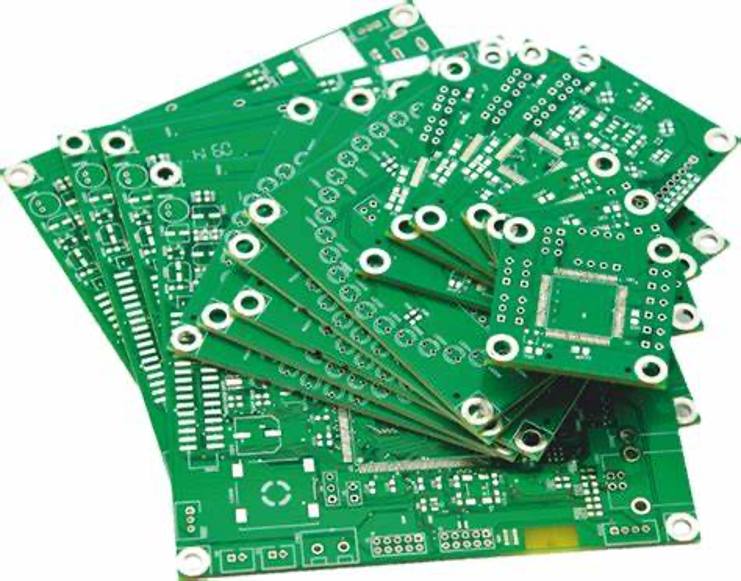
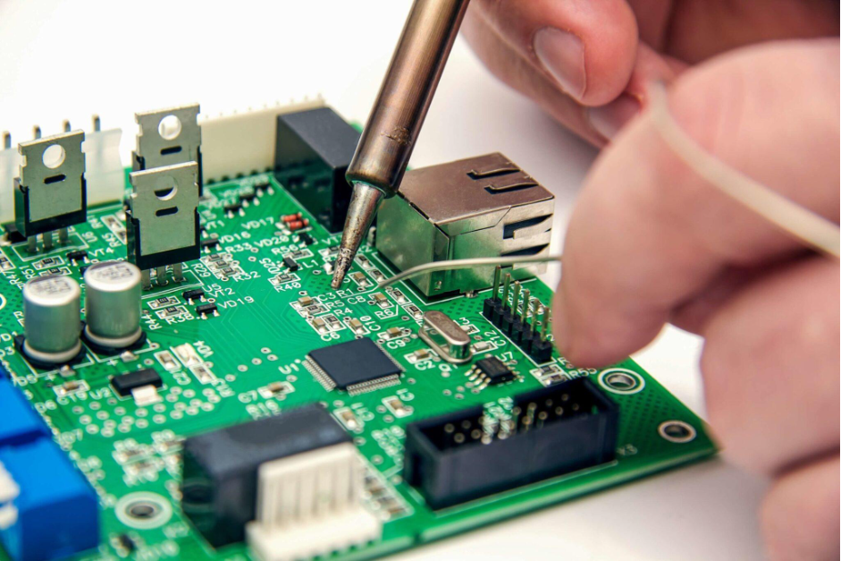
After the schematic and layout creation, PCB manufacturers print out the circuit board. Initially, the board is unassembled: it does not contain any components. The components are added further and the final result is an assembled circuit board – PCBA. Components should be ordered in advance: it will help to save time. Also, make sure that needed components are in stock. If you want to avoid all these troubles you can always hire a hardware design firm.
Finally, after all the components are placed on the PCB and reflowed, being permanently connected to the board, PCBA is tested for quality. The process of testing determines whether the components are connected and whether they are located and connected in accordance with the plan. There are various tests that are applied at this stage, for example, ICT (In-circuit test), AOI (Automatic Optical Inspection), X-ray, and others. The process of PCB design and manufacturing is complex and requires attention to detail. It is not enough just to print a circuit board and connect components. This process involves some supply chain management and planning. So, it seems rational to delegate the whole process to professionals that will easily design and create an assembled circuit board of high quality in time.